
The Future in
2D
In the Department of Physics, a group of researchers are working to understand how to design, build and use these unique materials, which show promise for improving the power, efficiency and storage of electronic devices.
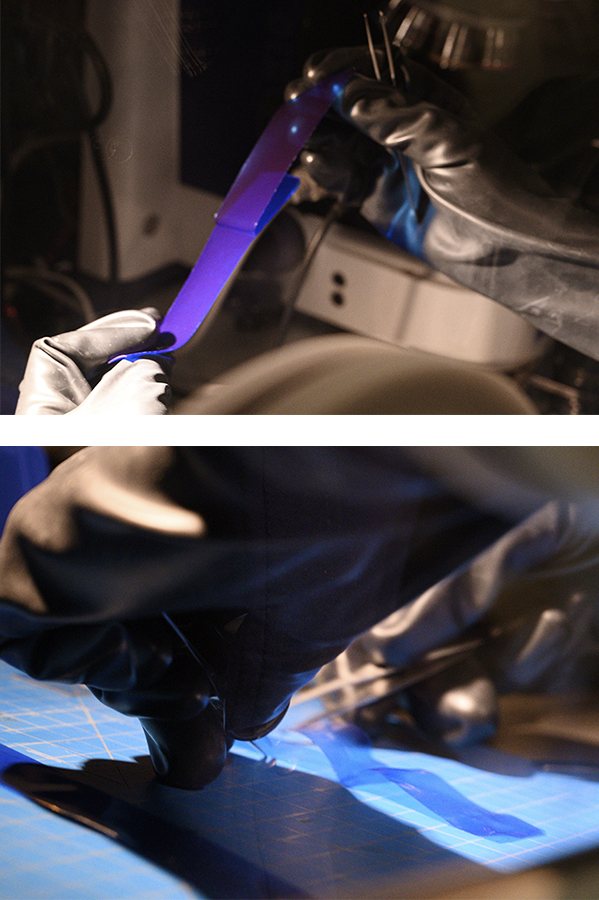
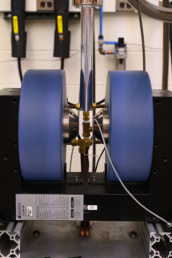
This team of 2D materials scientists is set to take the next big step in their research with the construction of a new quantum electronics laboratory in Wean Hall.
“It’s going to enable us to really throw everything we have in terms of experimental techniques at the most exciting 2D structures,” noted Assistant Professor Ben Hunt.
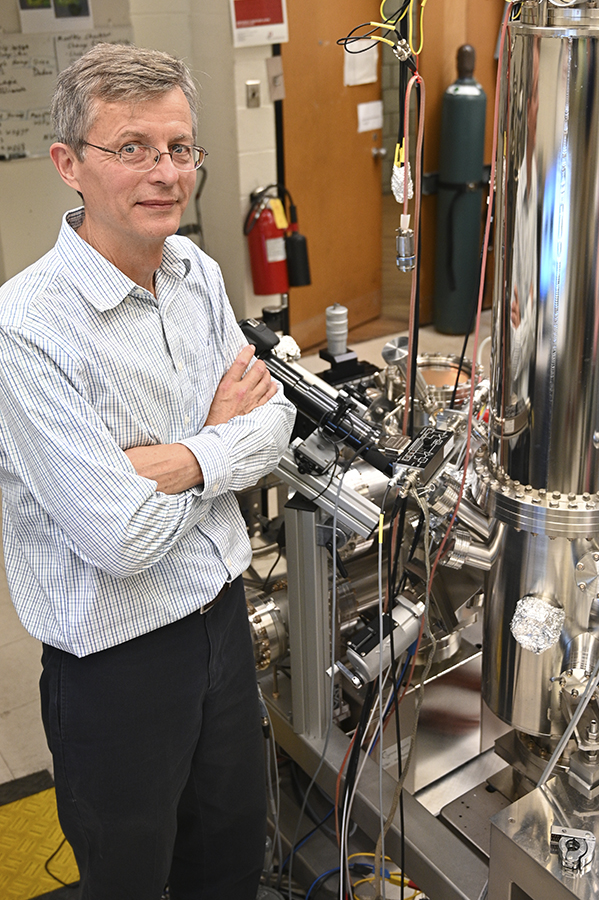
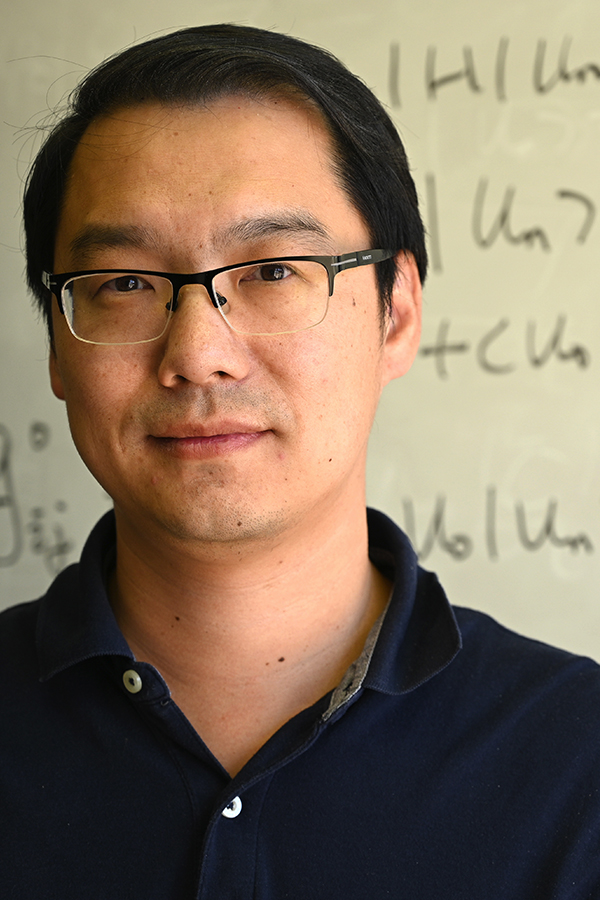
Randall Feenstra
“The goal is to really understand what the electrons are doing in these materials,” Professor Randall Feenstra said in describing his research.
In a 2D material, Feenstra explained, electrons are confined to moving around in a single plane. This can result in special effects, namely that electrons tend to move around more easily in two dimensions than in three, and that the influence of magnetism or voltage on the electrons is greater. The semiconductors found in nearly all modern electronic devices already confine electrons to a relatively thin layer of material to harness these effects, but none has yet to extend that confinement to a single atomic layer like in 2D materials.
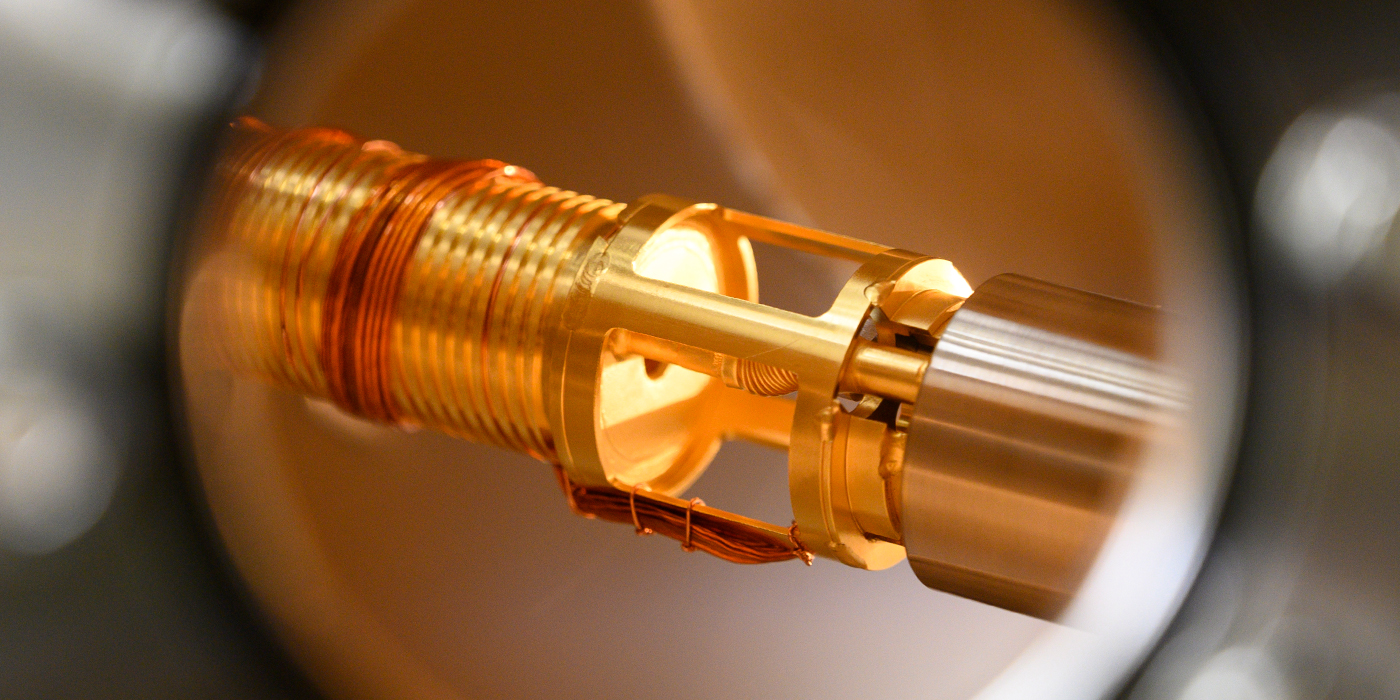
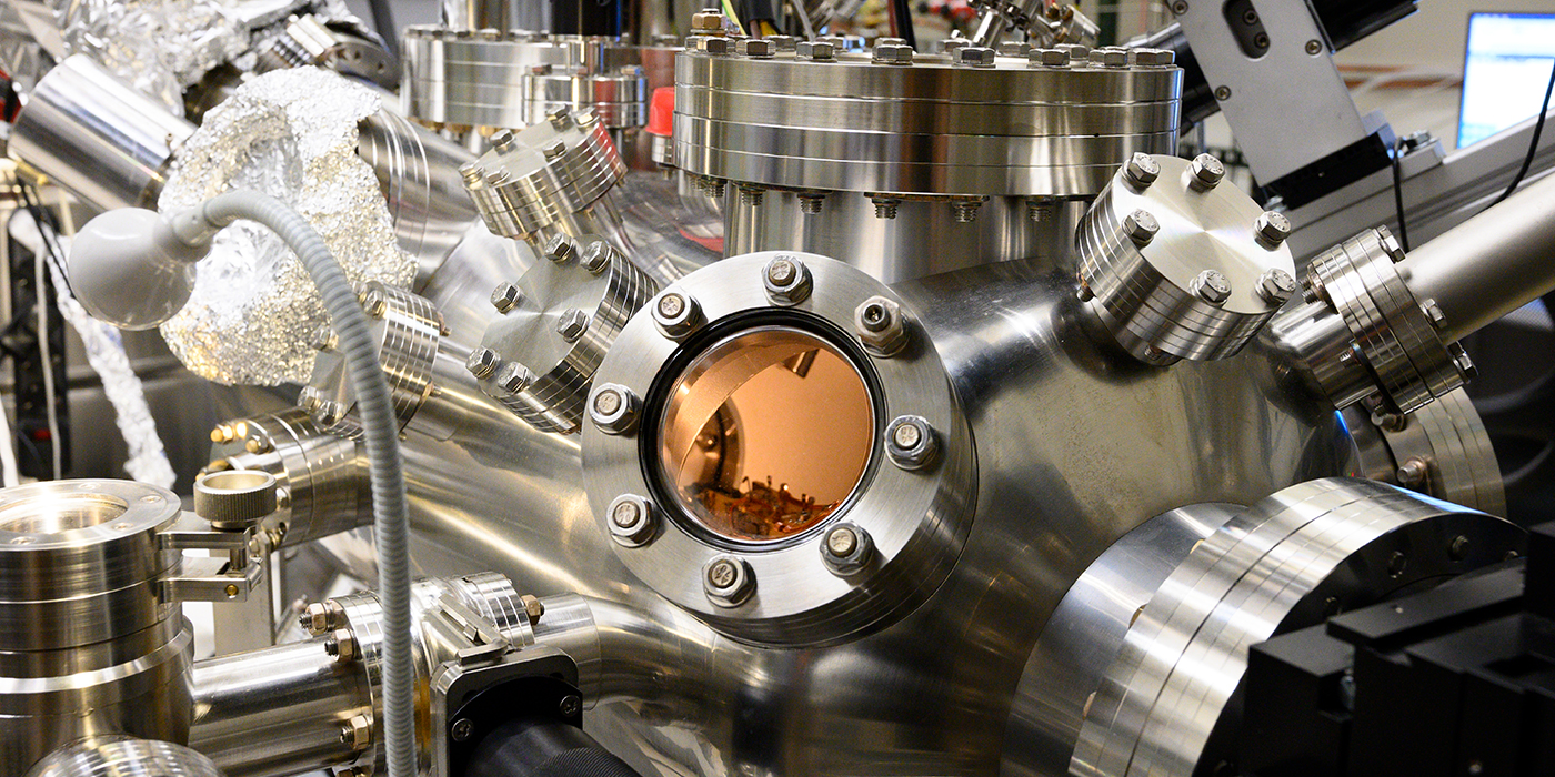
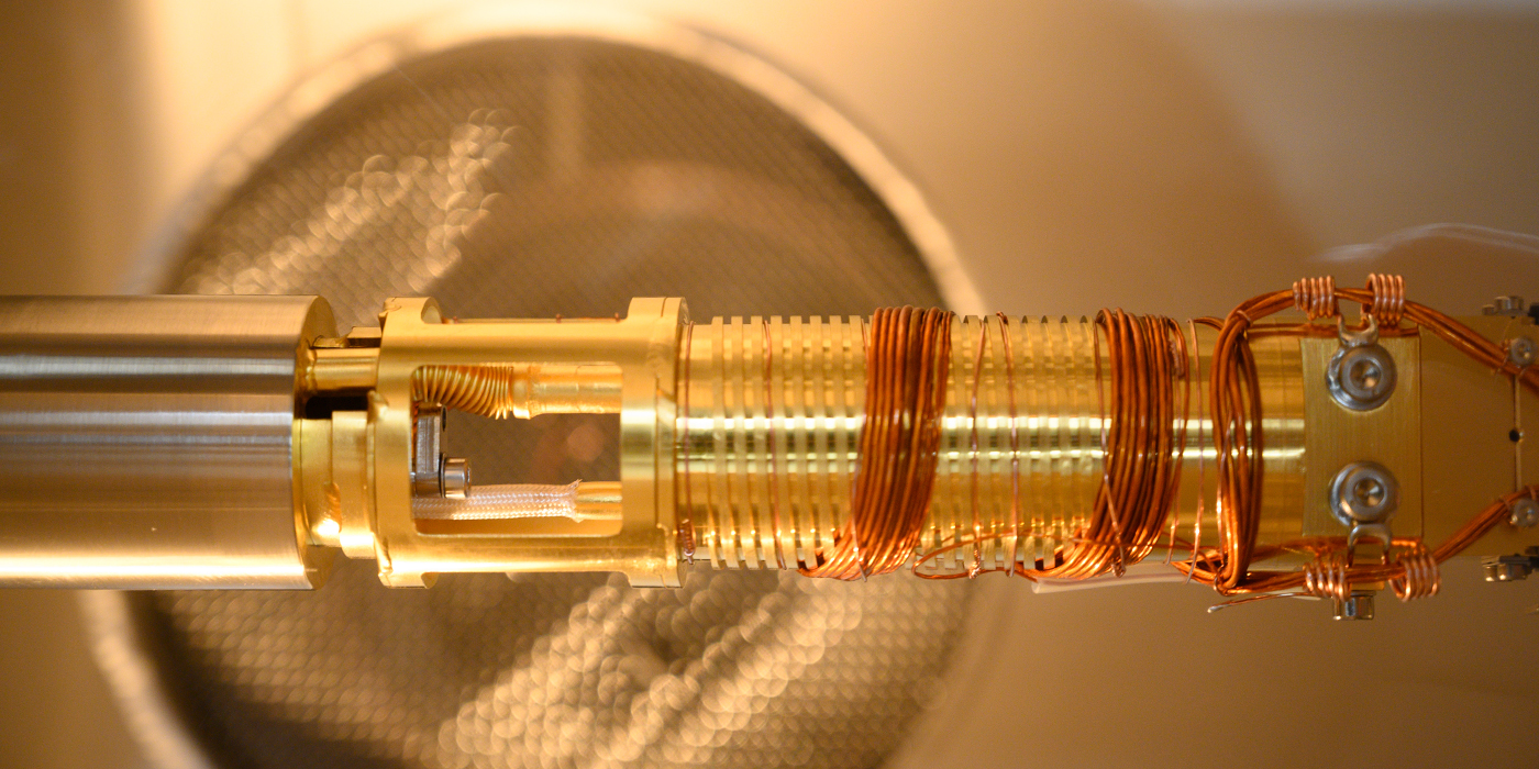
At Carnegie Mellon, Feenstra makes extensive use of a scanning tunneling microscope to study heterostructures that consist of layers of two-dimensional materials. “The electrons in one layer can affect the electrons in the layer below,” Feenstra noted, “or the electrons can move from one layer to the other.”
That latter effect, known as quantum tunneling, is predicted to be a key part of highly energy efficient transistors in the future.
“They’re super difficult to make,” Feenstra said, “but it would be wonderful if somebody could make those someday.”
“The world of practical devices is intimately connected with the physics world that we work in,” Feenstra said, noting his background as a researcher at IBM before coming to Carnegie Mellon in 1995. “We’re just looking for novel, sometimes exotic, ways in which the electrons move.”
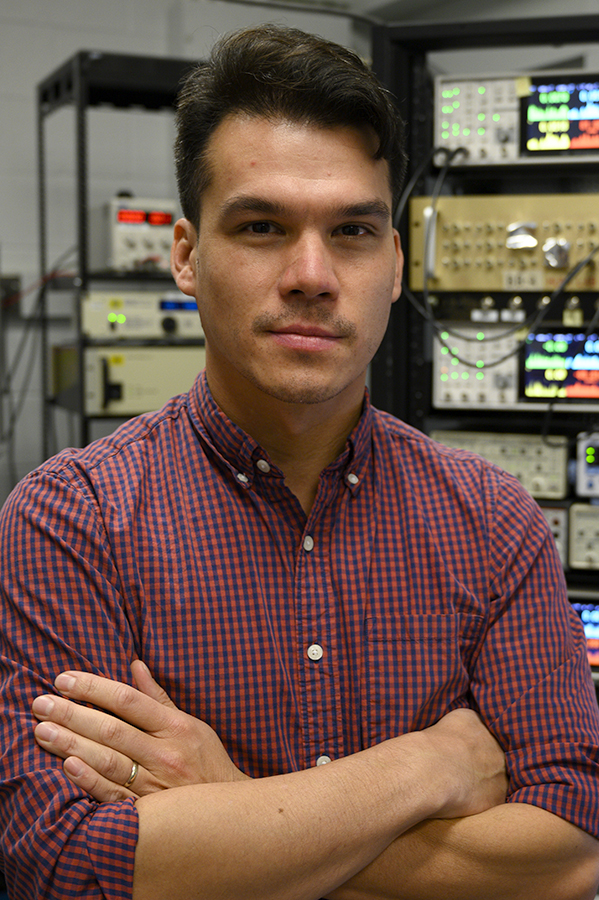
Ben Hunt
“My research in 2D materials is about what happens when we subject electrons to extreme conditions,” explained Hunt. In his lab, that means exposing materials to very low temperatures or powerful magnetic fields.
“Then, the quantum nature of the behavior of electrons really shines through,” Hunt said. “Electrons can do very, very surprising things when you get in that regime.”
Hunt hopes to harness those surprising electron actions to create better superconductors, which would allow the creation of more energy efficient and powerful electronic devices.
“Two-dimensional superconductivity resembles superconductivity in 3D,” Hunt said, “but it has a lot of unique aspects that we can leverage.”
In his lab, Hunt has been assisted by numerous undergraduate and graduate students from the Mellon College of Science and other CMU colleges. “It’s a field in which you can be very creative,” Hunt said in explaining what draws so many students to consider research in 2D materials. “You can essentially look up a few materials that you might be interested in and ask the question ‘what happens if I put one of them on top of the other?’”
An example of this is a recent collaboration between Hunt and Feenstra that saw them combine a 2D superconductor with a 2D topological insulator, a material in which electrons are only able to move along its surface.
“This system has a lot of potential to make more complicated structures — to realize new states of matter that have never been seen in 2D materials before,” Hunt said.
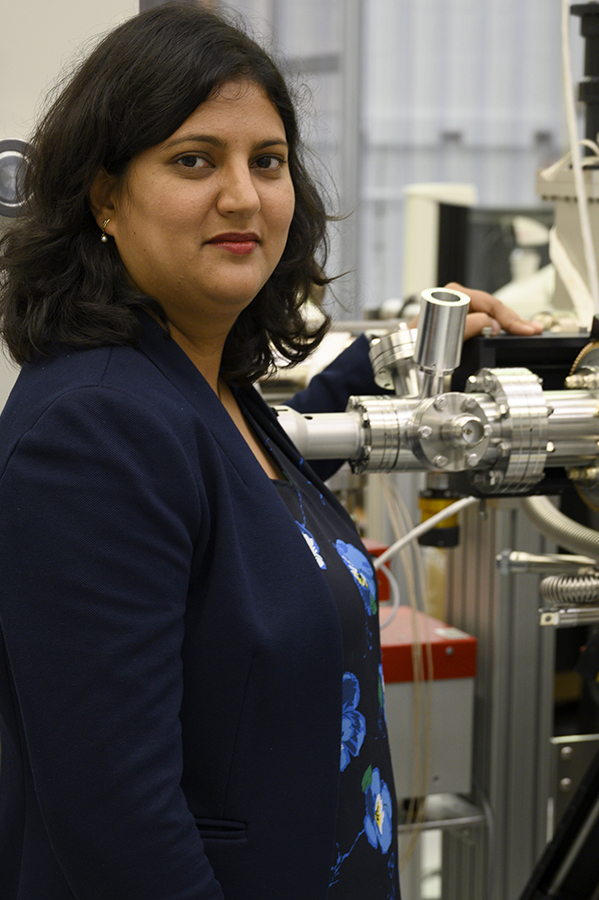
Jyoti Katoch
To Assistant Professor Jyoti Katoch, working with two-dimensional materials is a lot like building with Lego blocks.
“You can stack them vertically or horizontally,” Katoch explained. “You can build materials from the bottom up and can mix and match them and engineer the properties the way you want to, which has never been possible before.”
Katoch’s research seeks not only to understand the intrinsic properties that different combinations of 2D materials can give to heterostructures but also how external forces can affect them.
To achieve that, Katoch’s lab relies on a technique known as angle-resolved photoemission spectroscopy (ARPES), which can be used to observe the distribution of electrons, known as the band structure, in a material. While ARPES has been used widely for years, the size of the laser beams used for it has made the research method impossible to apply to observing very thin and small 2D materials. However, newer facilities have been able to focus ARPES lasers to nanometers in diameter, enabling researchers like Katoch to peer into the electronic band structures of 2D heterostructures.
“We are trying to really understand how the electrons behave and are arranged in these systems on a very basic level,” Katoch said.
Katoch has pushed nanoARPES even further by conducting in-operando measurements to track properties of electronic transport like conductivity while simultaneously observing the electron distribution in a 2D material. This advance can help her understand the underlying causes of changes in these properties in different heterostructures.
“Being able to correlate that transport measurement with the electronic band structure is something really unique,” Katoch said. “We can unlock all these mysteries.”
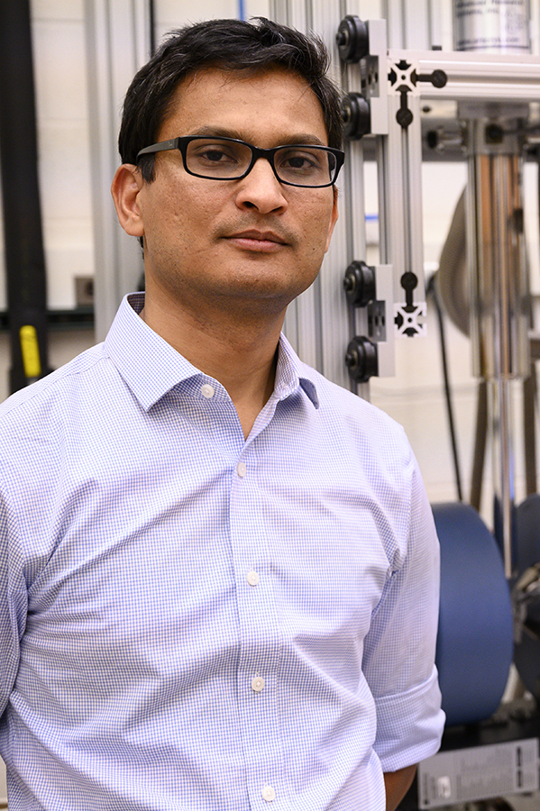
Simranjeet Singh
“My research focuses on understanding spin-related phenomenon in 2D materials,” said Assistant Professor Simranjeet Singh.
By spin, Singh is referring to a fundamental property of subatomic particles, such as electrons, that shows promise for being harnessed in electronic devices.
“Spin is as important as charge, and what you can do is encode information in these spins,” Singh said.
Traditional electronic devices, from supercomputers to smartphones, use charge to process and store bytes of information. However, being able to manipulate the spin of a particle enables another degree of freedom to exploit for computing or efficient data storage.
Extending this so-called spintronics could result in devices that store more information while using less power, Singh explains. His lab is currently focused on antiferromagnets — exotic materials with unique properties that make them promising for spintronics applications.
For example, writing data into storage in a normal electronic device already happens in nanoseconds, Singh explained, but storing the same information in an antiferromagnet can happen in one-trillionth of a second. Even more useful properties are likely to be created by making 2D versions of these materials, Singh noted.
“Two-dimensional antiferromagnets provide a tunable platform to study all these very interesting phenomena,” Singh said.
Singh and Katoch, who run their lab jointly, only came to Carnegie Mellon last year, but they already have numerous graduate and undergraduate students working in their lab, with more expressing interest every month.
“We have been getting a lot of emails,” Singh said. “It’s so cool that you can do these exciting things with these two-dimensional materials.”
Di Xiao
“In some ways our research is really like something every kindergartener can do,” Xiao said in explaining his lab’s work to predict and understand the properties of theoretical combinations of materials. “You put different materials together and you can get new functionalities.
“This sounds very simple, but it’s actually not,” Xiao said.
That’s because in the crystalline solids used to make semiconductors one has to not only consider how those materials would interact with each other, but also make sure that the 3D structure of the atoms in each material matches the other properly.
In two dimensions, however, that consideration isn’t needed.
“You can actually neatly just put one on top of the other and they will stay there and give you a beautiful interface and many interesting physical effects,” Xiao said.
One area of special interest for Xiao’s research is magnetic 2D materials that could be used in spintronic devices.
Electromagnetic fields are a crucial part of computing, but to generate a magnetic field, one traditionally needs to inject an electric current into a material. Much of the energy in an electric current, however, ends up being dissipated as waste heat when it passes through a material. This means that even though a powerful supercomputer could beat the world’s best chess players, it requires immense and inefficient amounts of energy to do so.
However, layering 2D materials could create a heterostructure with magnetic properties that could be altered without the need of a current.
“Right now, we’ve only scratched the tip of the iceberg in terms of the possibility of making new materials and discovering new physics,” Xiao said.
■ Ben Panko